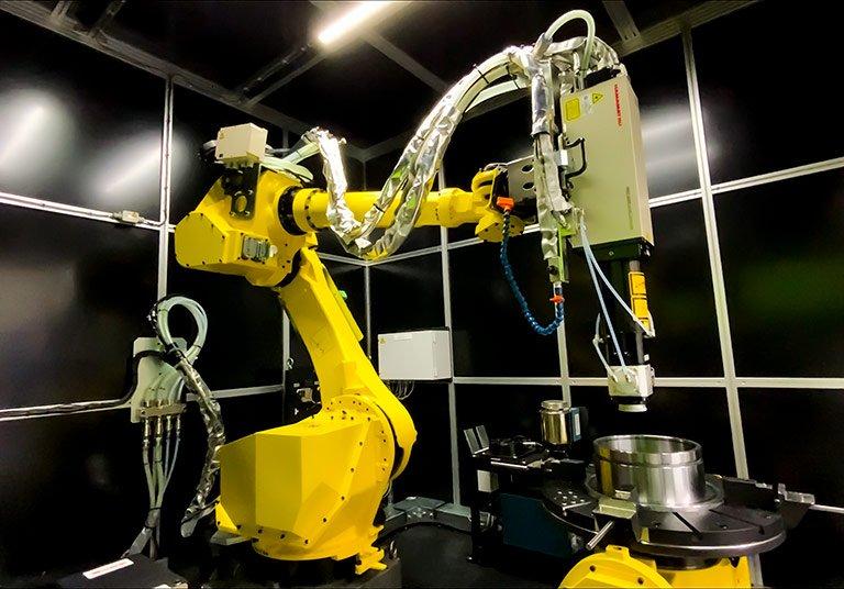
Hamamatsu Photonics has developed laser thermal processing equipment capable of operating with a high degree of freedom while emitting continuous to pulsed irradiation with a minimum pulse width of 4 milliseconds

At Hamamatsu Photonics we have developed laser thermal processing equipment for laser quenching that combines a direct diode laser, (DDL) that we newly designed and developed based on our unique laser diode (LD) technology, with a 6-axis robotic arm capable of operating with a high degree of freedom. This equipment irradiates a laser beam with […]

continue reading

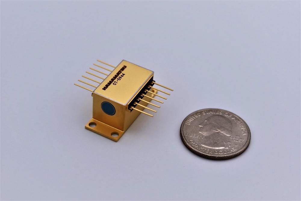
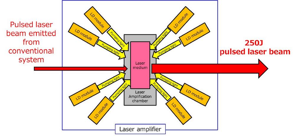
Hamamatsu Photonics develops an industrial pulsed laser system delivering the world’s highest output power of 250 joules!

Hamamatsu Photonics successfully developed an industrial pulsed laser system that produces a pulse energy of 250 J (joules) which is the world’s highest energy among LD-pumped lasers. The development of this laser system stems from the “Research and Development of Next Generation Laser Processing Technology” project supported by the NEDO, which is a national research […]

continue reading

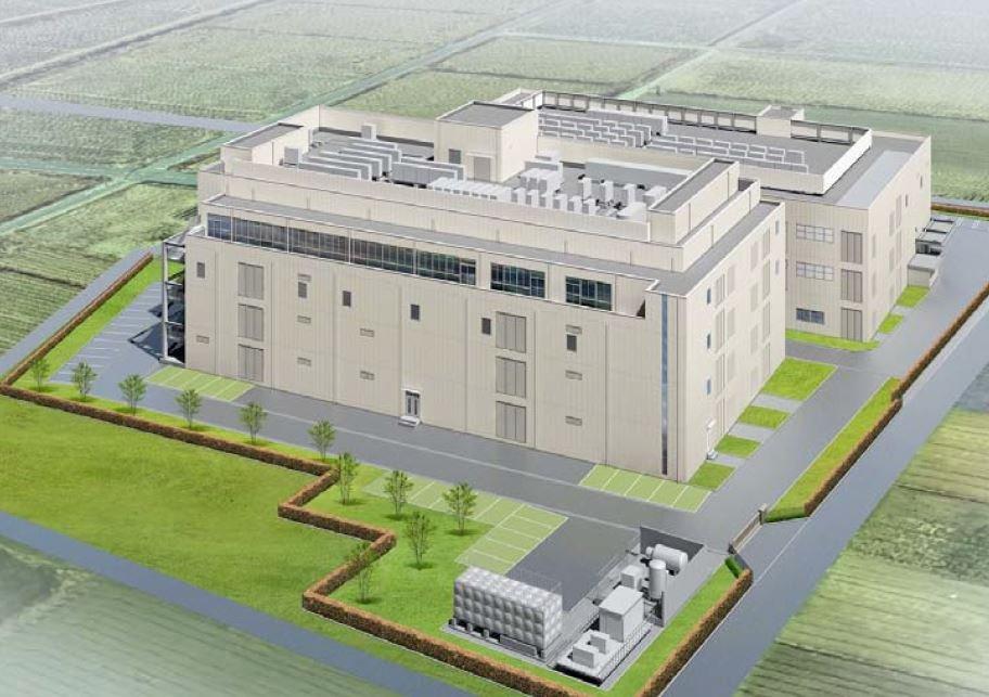
Koso Corporation, a production subsidiary of Hamamatsu Photonics, will be constructing a new factory building to boost its production capacity of electron tube light sources

Koso Corporation (677-1, Kakeshita, Iwata City, Shizuoka Prefecture, Japan) is a subsidiary of Hamamatsu Photonics which manufactures electron tube light sources. Koso Corporation will soon begin construction of a new factory Building No. 2 to boost production capacity. The groundbreaking ceremony for the new factory building will be held on Monday, August 2, 2021 and […]

continue reading

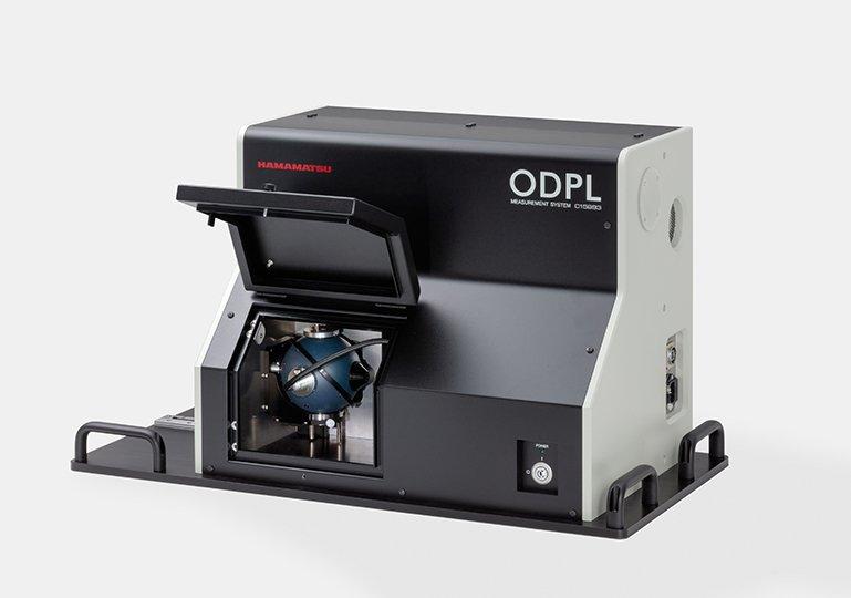
Hamamatsu Photonics has developed a GaN crystal evaluation system that uses ODPL spectroscopy to quantitatively evaluate GaN crystal quality

Hamamatsu Photonics has developed a GaN (gallium nitride) crystal evaluation system “ODPL (omnidirectional photoluminescence) measurement system C15993-01” that leverages ODPL spectroscopy along with our unique light detection technologies including optical design and data processing. This ODPL measurement system quantitatively evaluates the quality of GaN crystals that are currently drawing vast attention as a material for […]

continue reading

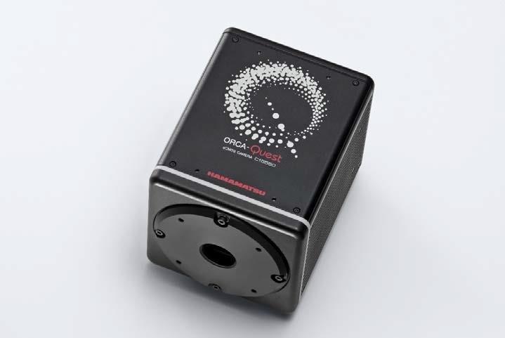
Hamamatsu Photonics introduces the world’s first photon-number-resolving scientific camera with incredibly low noise and 9.4 megapixels

Hamamatsu Photonics has designed and produced a scientific camera called the ORCA®-Quest qCMOSTM camera (part number C15550-20UP), having incredibly low noise of 0.27 electrons rms and a high pixel number of 9.4 megapixels. What makes this possible is a new two-dimensional CMOS (complementary metal-oxide semiconductor) image sensor, designed by applying our unique design technology and […]

continue reading

Hamamatsu Photonics will construct a new factory building at the Toyooka factory site to boost production capacity of its electron tube products

Hamamatsu Photonics will construct a new factory Building, No. 11, at its Toyooka factory site (Shimokanzo, Iwata City, Japan) to handle the increase in sales of Microfocus X-ray sources (MFX) and other electron tube products. The groundbreaking ceremony for the new factory building will be held on Wednesday 19 May 2021, and is scheduled to […]

continue reading

Hamamatsu Photonics launches a new Webinar: qCMOS

This webinar with Peter Seitz, Ph.D., will provide an overview of semiconductor image sensors and introduce photon-resolving quantitative CMOS imaging (qCMOS). Wednesday, May 19th at 5:00pm CEST, 11:00AM EDT Register: https://www.hamamatsu.com/eu/en/news/event/2021/20210519190000.html About this webinar: Imaging in general and semiconductor imaging in particular have penetrated every aspect of our lives, especially in the sciences. They have […]

continue reading

Hamamatsu Photonics will construct a new factory building at the Joko factory site to boost production capacity of image measurement devices and equipment business

Hamamatsu Photonics will construct a new factory, Building No. 5 at the Joko factory site (Joko-cho, Higashi-ku, Hamamatsu City, Japan) to handle expanding sales of image measurement devices and equipment such as digital cameras for scientific measurement, digital pathology slide scanners, and semiconductor failure analysis systems. The groundbreaking ceremony for the new factory building is […]

continue reading

Hamamatsu Photonics has developed laser thermal processing equipment capable of operating with a high degree of freedom

At Hamamatsu Photonics we have developed laser thermal processing equipment for laser quenching that combines a direct diode laser, (DDL) that we newly designed and developed based on our unique laser diode (LD) technology, with a 6-axis robotic arm capable of operating with a high degree of freedom. This equipment irradiates a laser beam with […]

continue reading