- Process innovation for through-glass vias in advanced packaging and display
- Launch at Touch Taiwan on April 19-21 in Taipei
Plan Optik AG (Elsoff, Germany) and 4JET microtech (Alsdorf, Germany) have jointly developed a process chain for the highly productive production of metallized through-glass vias.
The new VLIS process (short for Volume Laser Induced Structuring) enables the production of high-precision TGV ("Through Glass Vias") for advanced packaging in glass wafers, or substrates for displays.
TGV are micro-holes with a diameter of typically 10µm to 100µm. For various applications in the advanced packaging sector, tens of thousands of these vias are applied per wafer and metallized to produce the required conductivity. TGVs are also used in the manufacture of displays, for example based on µLED. Previous methods for manufacturing have been slow, associated with high reject rates, and difficult to match to the metallization process.
The teams from the two companies have now developed a solution that can prepare several 10,000 vias per minute, which are etched in a batch process for subsequent plating. The resulting channels are positioned with a hole-to-hole accuracy better than +/- 2µm, the substrates are free of microcracks, and the insides of the channels are smooth-walled and can be homogeneously metallized. The process is suitable for glass types typical in the semiconductor and display industry. In addition to glass starting thicknesses of 100µm, various copper layers down to 25µm thickness can be realized.
The two partners have agreed on a cooperation that provides users with a high degree of flexibility: Customers can either purchase components produced with VLIS from Plan Optik, or purchase qualified total solutions for system technology including laser systems, wet chemistry and metallization from 4JET and partners.
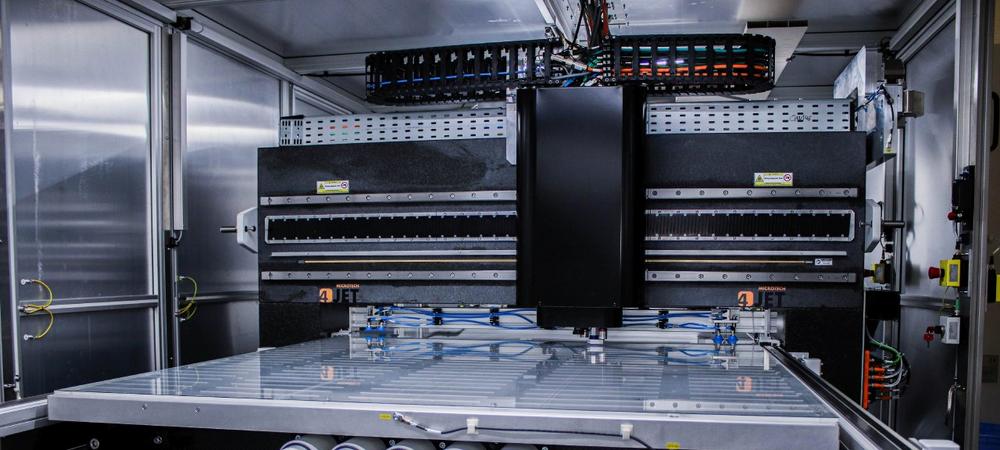
Plan Optik already has a modern production chain for the manufacture of glass wafers and masters all process steps from wafer cutting and edge processing, through structuring and cleaning, to metallization. The addition of 4JET’s system technology now enables the rapid and positionally accurate modification of substrates. A modified version of the proven 4JET laser systems for cutting glass is used. The PEARL platform is already used for cutting glass substrates in display, architectural glass, or medical technology. Depending on the version, the systems are capable of high-precision modification of glasses up to 2.2 m x 3 m.
A New Technology
The use of laser technology for selective etching is not new, but overall the cooperation delivers significant advances for customers: the combination with Plan Optik AG’s extensive process chain creates the world’s leading solution chain for fully processed and metallized TGV wafers. At the same time, the precision, speed and availability now achievable on very large substrates enables application in display manufacturing for the first time.
The two partners see further potential for the VLIS process for glass-based MEMS, microfluidics or high-frequency antenna technology (e.g. 6G)
The PEARL systems are based on a granite machine platform that offers inherent accuracy and long-term stability. Cutting geometries and positions for interposers can be easily imported from CAD drawings. Targeted tuning of axis controls results not only in high cutting speed, but also in excellent path accuracy to achieve high-precision machining. The PEARL DYNAMIC FOCUS ensures that the focus is always within the process window without increasing process time.
About Plan Optik
As a technology leader, Plan Optik AG produces structured wafers at locations in Germany and Hungary. These wafers are indispensable as active elements for numerous microsystem technology applications in industries such as consumer electronics, automotive, aerospace, chemicals and pharmaceuticals. The wafers, made of glass, glass-silicon or fused silica, are offered in diameters of up to 300 mm. Wafers from Plan Optik offer high-precision surfaces in the Angstrom range (= ten millionths of a millimeter), which are achieved by using the MDF polishing process developed in-house. With its subsidiaries Little Things Factory GmbH and MMT GmbH, Plan Optik is also active in the field of microfluidics and lab-on-chip, where it is one of the few suppliers of complete systems. This business area is finding more and more applications, for example in medicine and chemistry, and thus offers similarly high growth potential as the area of the previous core business of wafer technology. The shares of Plan Optik AG are listed on the Open Market (Basic Board) of the Frankfurt Stock Exchange.
About 4JET
Alsdorf-based 4JET Group delivers solutions for the surface technology of the future. The company was founded in 2006 and employs 180 people, including over 80 engineers and developers. Customers include all of the world’s leading tire manufacturers, numerous automotive suppliers and OEMs, as well as the largest manufacturers of flat glass and thin-film photovoltaic cells. The company, headquartered in Alsdorf near Aachen, also operates a job store for technical glass processing and has subsidiaries in Shanghai and Atlanta.
For more information, visit www.4jet.de.
Alsdorf-based 4JET Group delivers solutions for the surface technology of the future. The company was founded in 2006 and employs 180 people, including over 80 engineers and developers. Customers include all of the world’s leading tire manufacturers, numerous automotive suppliers and OEMs, as well as the largest manufacturers of flat glass and thin-film photovoltaic cells. The company, headquartered in Alsdorf near Aachen, also operates a job store for technical glass processing and has subsidiaries in Shanghai and Atlanta.
For more information, visit [url=https://www.4jet.de/en/]www.4jet.de/en/[/url]
The 4JET Group
Otto-Lilienthal-Straße 1
52477 Alsdorf
Telefon: +49 (2404) 9221-0
Telefax: +49 (2404) 9221-133
http://www.4jet.de
Marketing Manager
Telefon: +49 (2404) 9221-0
Fax: +49 (2404) 9221-133
E-Mail: Elke.Blome@4jet.de
![]()

