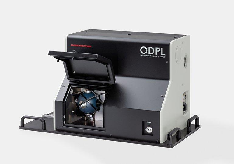
Sales of this new ODPL measurement system start on Monday, August 2, 2021 for researchers at universities and semiconductor substrate manufacturers both in Japan and overseas. The system will be presented at the “SEMI Partner Search – For Power & Compound” on-line event, which is scheduled to take place Wednesday, July 14, 2021.
ODPL spectroscopy
ODPL spectroscopy is a novel technique for quantifying and accurately evaluating the quality of compound semiconductor crystals such as GaN by quantifying structural defects and impurities within the crystal.
In traditional measurement methods utilizing photoluminescence (PL)(*1), the quality of semiconductor crystals such as GaN is evaluated based on the intensity and wavelengthspecific information of PL emitted in one direction from a sample crystal. Photoluminescence measurement methods allow rapid non-contact and non-destructive evaluation of crystal quality. However, these methods have issues such as poor reproducibility and poor quantitative determination because measurement results depend on the detector position and angle and also on conditions for irradiating the crystal with light.
Against this backdrop, in 2016, Hamamatsu Photonics and a research group from the Institute of Multidisciplinary Research for Advanced Materials at Tohoku University headed by Associate Prof. Kazunobu Kojima and Prof. Shigefusa Chichibu succeeded in making highly reproducible measurements of PL intensity emitted in all directions from a GaN crystal by using an integrating sphere (*2). At the same time, this allowed us to discover that the internal quantum efficiency (IQE)(*3) of GaN crystals could be calculated from the measurement results by also using our unique calculation method. Then, using the IQE of the GaN crystals as an index, we established an ODPL spectroscopy measurement method for quantitatively evaluating the crystal quality.
*1. PL or photoluminescence is the light emitted when electrons and holes, which are generated within a semiconductor by irradiation of light with an energy state higher than the band gap of the semiconductor material, recombine and return to the original state.
*2: An integrating sphere is a hollow spherical shell coated on its inner surface with highly reflective material. The total luminous flux of light emissions generated by a light source in the sphere can be obtained by spatially integrating and detecting the light reflected in the integrating sphere.
*3: IQE or internal quantum efficiency is the probability that the energy absorbed by a material is converted to photons.
Product overview
This ODPL measurement system accurately evaluates GaN crystal quality by utilizing ODPL spectroscopy.
Hamamatsu Photonics designs, manufactures and sells sophisticated devices that measure luminous efficiency based on the PL emitted from luminescent materials. Hamamatsu has now applied its long-fostered light detection and optical design technologies to create new software for this purpose. It not only accurately measures the PL intensity emitted in all directions from GaN crystals via an integrating sphere but also automatically calculates the IQE based on the measurement results. This in turn led us to successfully develop an ODPL measurement system that quantitatively evaluates GaN crystal quality by ODPL spectroscopy. We also optimized the placement of optical components to make the equipment components such as the integrating sphere, monochromator and optical systems more compact. A newly developed sliding sample holder is also provided to make it easier to place the GaN crystal.
Since the ODPL measurement system can quantitatively evaluate the GaN crystal quality by using ODPL spectroscopy, it will serve as a powerful tool that vastly boosts efficiency of R&D work on improving GaN crystal quality.
We plan to keep expanding sales of this ODPL measurement system and make an industry standard of ODPL spectroscopy measurements for quantitative evaluation of GaN crystal quality. We will also continue to design ever more versatile equipment that supports larger GaN crystal wafers to help streamline the quality inspection process on future mass production lines.
Major features
1. Quantitative evaluation of GaN crystal quality
Hamamatsu Photonics and the research group headed by Associate Prof. Kazunobu Kojima and Prof. Shigefusa Chichibu at the Institute of Multidisciplinary Research for Advanced Materials of Tohoku University quantified GaN crystal quality in terms of structural defects and impurities by calculating the IQE of GaN crystals with the aid of measurement technology utilizing an integrating sphere and our unique calculation method. We then established an ODPL spectroscopy measurement method for accurately evaluating crystal quality. The ODPL measurement system that we succeeded in developing utilizes ODPL spectroscopy to quantitatively evaluate the GaN crystal quality and also relies heavily on our long-fostered light detection, optical design and data processing technologies.
2. Compact and user-friendly configuration
We also optimized the optical component placement to make the equipment more compact. A newly designed sliding sample holder also makes it easier to place GaN crystals during measurement.
Development background
In fields such as electronic devices, rail transport, and next-generation automobiles including EV, the demand for power semiconductors that can control power more efficiently than ordinary semiconductors are rapidly growing. Recently, next-generation power semiconductors made from GaN crystals are drawing serious attention as the key to further downsizing and higher speed. Quality evaluation of those power semiconductors is becoming more and more important, yet their quality cannot be quantitatively rated by conventional methods. Therefore, we have been working to develop semiconductor crystal evaluation systems capable of quantitatively evaluating GaN crystal quality.
Hamamatsu Photonics Deutschland GmbH
Arzberger Str. 10
82211 Herrsching am Ammersee
Telefon: +49 (8152) 375-0
Telefax: +49 (8152) 375-199
http://www.hamamatsu.com
Public Relations
Telefon: +49 (8152) 375-185
Fax: +49 (8152) 375-199
E-Mail: rfritsch@hamamatsu.de
![]()

