“We are delighted to be working with Fraunhofer IISB within this new initiative,” said Bruce Hueners, CEO and President for Palomar Technologies and SST Vacuum Reflow Systems. “Palomar Technologies works with research institutes around the world to contribute to the development and advancement of techniques and technologies key to microelectronics packaging for the semiconductor industry. The work with these institutes results in new processes, new products, or new applications for industry.”
Fraunhofer IISB conducts applied research and development in the field of electronic systems for application in, e.g., electric mobility, aerospace, Industry 4.0, power grids, or energy technology. In this connection, the institute uniquely covers the entire value chain – from basic materials to whole power electronic systems.
“The packaging technologies are essential for cost effective and reliable power electronics. They offer the potential for improvements in every single domain. This cooperation will allow us to create significant progress in the field of solder materials and processing,” explained Andreas Schletz, head of the department for devices, packaging, and reliability at Fraunhofer IISB.
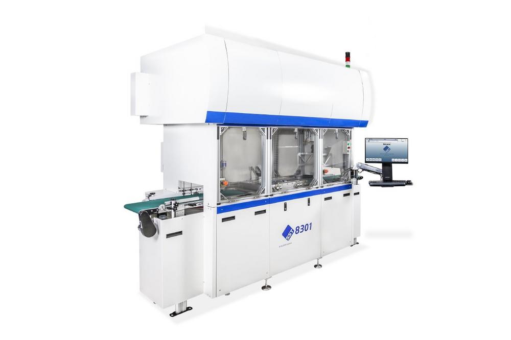
As part of the cooperation, Palomar will place a SST 8301 Automated Vacuum Soldering System within the Fraunhofer Institute. It will be available for demonstrations, prototypes, and research projects focusing on key components inside power electronics, dies to DBC, connectors/pins to DBC and DBC to base plate soldering. The SST 8300 Series Automated Vacuum Pressure System offers superior bond technology for soldering and/or sintering processes. The entire process takes place in a single chamber with a single process profile, however, additional chambers can be added or upgraded in the field as production capacity needs increase.
Today, the SST 8301 is the only solution to use both vacuum pressure and pressure above atmospheric, serving to drive voids close to zero. This technology solves the key problem of voiding and thermal mismatches with the larger surface area attachments in the critical DBC to Baseplate joint. The 8301 is capable of a reliable flux-less soldering with less than 1% voiding, significantly improving yielded throughput.
To learn more about the research initiative, visit
https://www.palomartechnologies.com/research-initiative-fraunhofer-iisb
or the Fraunhofer Institute for Integrated Systems and Device Technology IISB
https://www.iisb.fraunhofer.de/packaging.
About Palomar Technologies
Palomar Technologies makes the connected world possible by delivering a Total Process Solution™ for advanced photonic and microelectronic device assembly processes utilized in today’s smart, connected devices. With a focus on flexibility, speed, and accuracy, Palomar’s Total Process Solution includes Palomar die bonders, Palomar wire and wedge bonders, SST vacuum reflow systems, along with Innovation Centers for outsourced manufacturing and assembly, and Customer Support services, that together deliver improved product quality and yield, reduced assembly times, and rapid ROI.
With its deep industry expertise, Palomar equips customers to become leaders in the development of complex, digital technologies that are the foundation of the connected world and the transmission of data generated by billions of connected devices. Palomar solutions are utilized by the world’s leading companies providing solutions for datacom, 5G, electric vehicle power modules, autonomous vehicles/LiDAR, enhanced mobile broadband, Internet of Things, SMART technology, and mission-critical services.
Headquartered in Carlsbad, California, Palomar offers global sales, service and application support from its offices in the USA, Germany, Singapore, and China.
For more information, visit: http://www.palomartechnologies.com
As one of the 74 institutes and research units of the Fraunhofer-Gesellschaft, the Fraunhofer Institute for Integrated Systems and Device Technology IISB conducts contract research for industry and public authorities. Its main objective is to provide excellent research to its customers and to set technological benchmarks as one of the leading research institutions in electronic systems. For this, about 250 employees plus numerous students work on a broad range of power electronics for mobility, industry, and energy supply, semiconductor devices and technology, packaging and modules, and materials development. This is supplemented by broad activities in test and reliability, simulation, characterization, and metrology.
In addition to silicon technology, the IISB has a strong focus on wide-bandgap semiconductors, especially silicon carbide (SiC). For SiC, the institute offers a complete technology backbone, including materials science, devices, modules, and their integration in highly efficient power electronic systems.
Besides its headquarters in Erlangen, Fraunhofer IISB has branches in Nuremberg and Freiberg / Saxony. The institute closely cooperates with the Friedrich-Alexander-Universität Erlangen-Nürnberg (FAU) and is a foundation member of the "Energie Campus Nürnberg" (EnCN) as well as the "Leistungszentrum Elektroniksysteme" (LZE). IISB pursues cooperation with numerous national and international partners in joint projects and associations.
For more information on IISB, see: https://www.iisb.fraunhofer.de/
Fraunhofer-Institut für Integrierte Systeme und Bauelementetechnologie IISB
Schottkystraße 10
91058 Erlangen
Telefon: +49 (9131) 761-0
Telefax: +49 (9131) 761-390
http://www.iisb.fraunhofer.de
Packaging Technologies
Telefon: +49 9131 761 215
E-Mail: christoph.bayer@iisb.fraunhofer.de
![]()

